- Home
- India: The Emerging Design Hub for the Global Semiconductor Industry
India: The Emerging Design Hub for the Global Semiconductor Industry

Introduction:
The global semiconductor landscape is undergoing a fundamental shift. With increasing geopolitical tensions, rising costs, and the need for supply chain resilience, companies in the US, Europe, and East Asia are reassessing their strategies for chip design and innovation.
In this context, India is rapidly emerging as a credible and strategic destination for semiconductor design and development. Fueled by government policy support, a skilled workforce, and an expanding technology ecosystem, India is not just a cost-effective option—it is a long-term growth partner for the global semiconductor industry.
Why Global Semiconductor Companies Are Looking to India
1. Rich and Scalable Engineering Talent
India produces hundreds of thousands of electronics and computer science engineers each year. This talent has powered design centers for companies like Intel, AMD, NXP, Qualcomm, and STMicroelectronics. Today, this workforce is equipped to support:
• Advanced VLSI design and verification
• System-on-chip (SoC) and ASIC development
• AI/ML accelerators, datacenter chips, and automotive electronics
• Embedded systems, firmware, and post-silicon validation
2. Government-Backed Semiconductor Policies
India has committed over ?76,000 crore (~$10 billion) under the Semicon India Programme to strengthen every part of the semiconductor value chain.
Key schemes include:
1. Design Linked Incentive (DLI) Scheme
• Reimburses up to 50% of eligible design expenditures.
• Open to both domestic and global players who register a business in India.
• Encourages co-development and technology partnerships.
2. Modified Semiconductor Fab Scheme
• Capital support up to 50% for companies establishing fabs in India.
• Applicable to logic, analog, and compound semiconductor nodes.
3. Support for OSAT/ATMP Units
• Focus on enabling high-volume, advanced packaging and testing capabilities.
• Complements design firms and helps close the loop locally.
4. India Semiconductor Mission (ISM)
• Coordinates ecosystem development, infrastructure, and global alliances.
• Acts as a single-window interface for large-scale semiconductor investments.
These schemes create a policy environment where global companies can build sustainable, IP-secure, and future-ready operations in India.
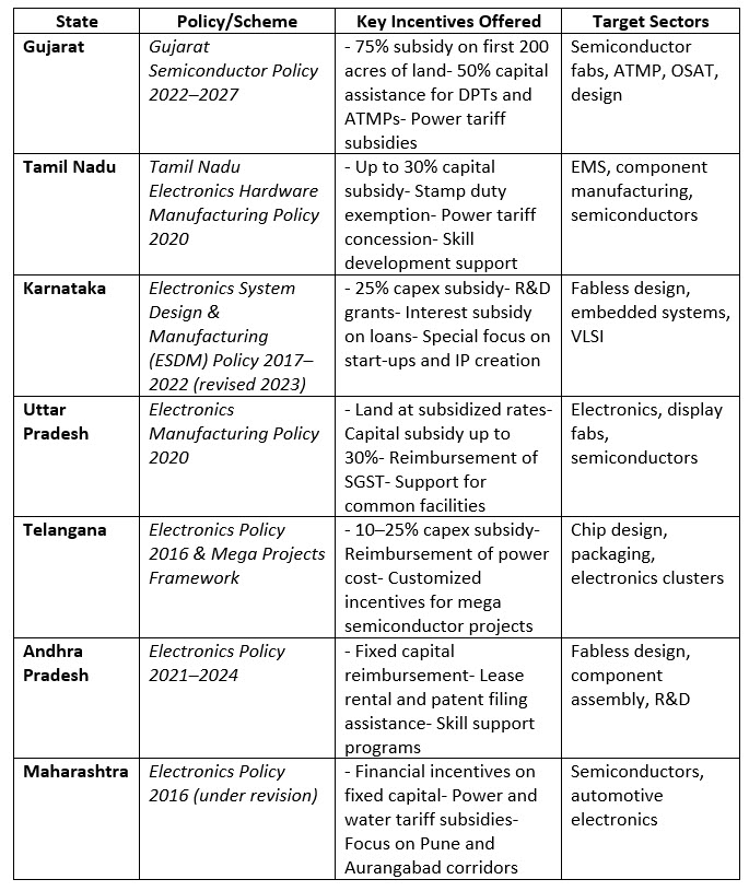
5. State-Level Incentives Supporting Semiconductor and Electronics Ecosystem in India
Strategic Advantages for UK, European and American Companies
Geopolitical Diversification
India offers an alternative to the East Asia-centric semiconductor model. With its democratic governance, rule of law, and alignment with Western regulatory frameworks, India is a strategically safe partner.
Optimised Cost with Global-Standard Quality
Engineering operations in India are 40–60% more cost-efficient than in Western markets, with no compromise on:
• Process maturity
• Toolchain familiarity (Synopsys, Cadence, Siemens EDA)
• IP confidentiality
Mature and Collaborative Ecosystem
India hosts:
• 100+ semiconductor design services firms
• ESDM clusters in Bengaluru, Hyderabad, Gujarat, and Noida
• Research partnerships with IITs, IISc, and private labs
• Active industry platforms like IESA and SCL
Strong IP and Data Security Regime
India’s legal framework is fully compliant with TRIPS and WIPO conventions. Foreign companies can:
• Register and protect patents in India
• Execute enforceable NDAs and licensing contracts
• Operate in ISO 27001-certified environments for IP-sensitive development
UK–India Free Trade Agreement: A New Gateway for Semiconductor Partnerships
On May 6, 2025, the United Kingdom and India officially signed a landmark Free Trade Agreement (FTA) aimed at deepening economic cooperation across key sectors, including semiconductors, advanced manufacturing, and technology services.
Key Benefits for the Semiconductor Industry:
- Reduced Tariffs: Lower import/export duties on semiconductor equipment, materials, and components, facilitating smoother trade between both countries.
- Encouragement of Joint Ventures: Policy clarity and investment protection mechanisms to support UK-India semiconductor R&D and co-design initiatives.
- Talent Mobility: Provisions for professional exchange programs and easier cross-border talent collaboration in high-tech sectors like chip design and electronics.
- Innovation Acceleration: FTA provisions include promotion of IP co-development and technology transfer, aligned with India’s Design Linked Incentive (DLI) and other schemes.
This agreement creates a compelling reason for UK-based chip design firms, IP vendors, and fabless startups to consider India not only for cost-effective engineering but also as a strategic partner aligned by policy and ambition.
As the UK seeks to diversify its semiconductor value chain and build innovation-led partnerships, India—with its policy incentives, skilled workforce, and design ecosystem—is now more accessible than ever.
Caliber Interconnect: Your Co-Innovation Partner in India
With India rising as a strategic design destination, and with Caliber at your side, you gain not just an outsourcing vendor—but a co-innovation partner.
Whether you are designing the next:
• AI accelerator,
• Electric vehicle controller,
• Hyperscale datacenter chip,
Caliber offers proven expertise in VLSI, ASIC/SoC development, verification, and embedded engineering—delivered from India, built for the world.
We work alongside global companies to scale innovation, reduce time-to-market, and ensure first-pass silicon success.
Conclusion: India’s Moment in Semiconductors Is Now
India is not just catching up—it is building a foundation for the future of semiconductors. The combination of policy push, talent depth, and global readiness makes it one of the most attractive destinations for strategic semiconductor partnerships.
For European and American companies seeking secure, skilled, and scalable design capabilities, India offers unmatched value—and firms like Caliber stand ready to collaborate.
Let’s Explore Possibilities
Whether you’re an OEM, fabless player, or technology partner—India has a role to play in your roadmap.
Connect with us to explore partnerships, design acceleration, and strategic collaborations.
Sources & Disclaimer
- The information presented in this article is intended solely for general reference and educational purposes. It has been compiled from publicly available government and industry resources, including:
• India Semiconductor Mission (ISM)
• Ministry of Electronics and Information Technology (MeitY)
• Invest India
• State Government Portals:
o Gujarat DST
o Karnataka ITBT
o ELCOT – Tamil Nadu
o UP IT & Electronics
o Invest MP
• Industry bodies such as IESA and NASSCOM
• Technology news portals like Economic Times and Electronics For You
• gov.uk Press Release : UK concludes trade deal with India
Disclaimer:
While efforts have been made to ensure the accuracy and relevance of the content, readers are advised to refer to official government notifications, websites, and policy documents for the latest and most authoritative information regarding semiconductor policies, incentives, and guidelines in India.